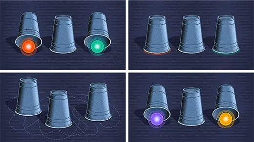
Physics Duo Finds Magic in Two Dimensions

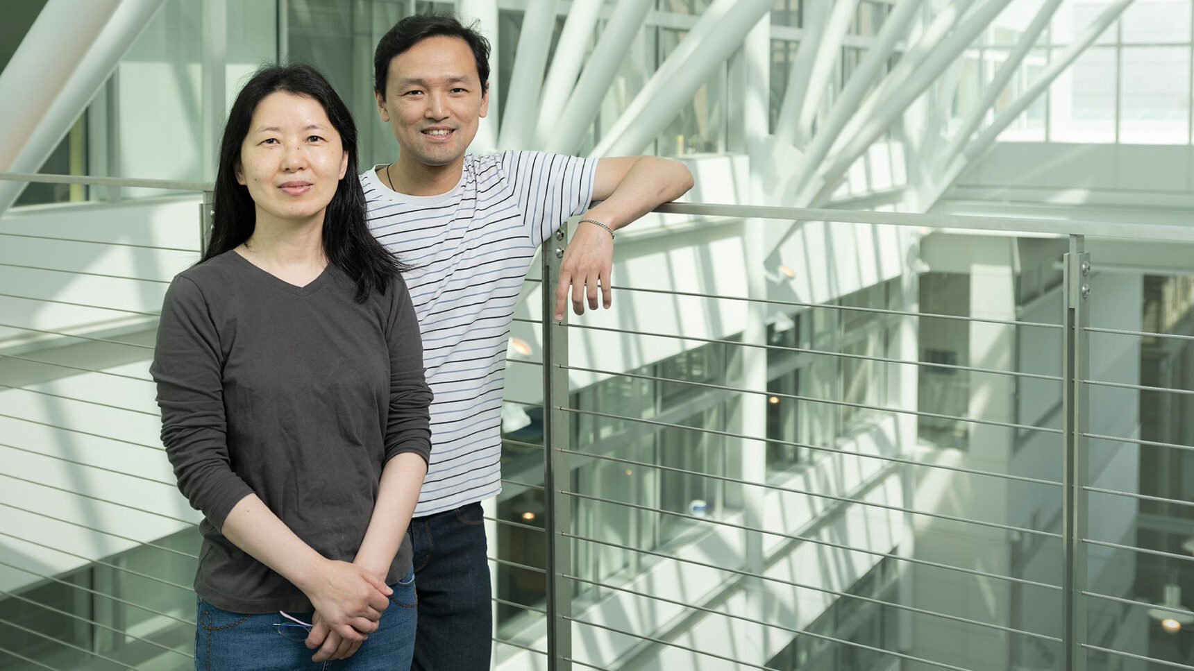
Of his partnership with Jie Shan (left), Kin Fai Mak said, “One plus one is more than two.”
Sasha Maslov and Olena Shmahalo for Quanta Magazine
Introduction
Molybdenite, even to the trained eye, looks almost identical to graphite — a lustrous, silvery crystal. It acts similarly too, sloughing off flakes in a way that would make for a good pencil filling. But to an electron, the two grids of atoms form different worlds. The distinction first entered the scientific record 244 years ago. Carl Scheele, a Swedish chemist renowned for his discovery of oxygen, plunged each mineral into assorted acids and watched the lurid clouds of gas that billowed forth. Scheele, who eventually paid for this approach with his life, dying of suspected heavy metal poisoning at 43, concluded that molybdenite was a new substance. Describing it in a letter to the Royal Swedish Academy of Science in 1778, he wrote, “I refer here not to the commonly known graphite that one can acquire from the apothecary. This transition metal seems to be unknown.”
With its tendency to flake into powdery fragments, molybdenite became a popular lubricant in the 20th century. It helped skis glide farther through the snow and smoothed the exit of bullets from rifle barrels in Vietnam.
Today, that same flakiness is fueling a physics revolution.
The breakthroughs started with graphite and Scotch tape. Researchers discovered by chance in 2004 that they could use tape to peel off flakes of graphite just one atom thick. These crystalline sheets, each a flat array of carbon atoms, had astonishing properties that were radically different from those of the three-dimensional crystals they came from. Graphene (as its discoverers dubbed it) was a whole new category of substance — a 2D material. Its discovery transformed condensed matter physics, the branch of physics that seeks to understand the many forms and behaviors of matter. Nearly half of all physicists are condensed matter physicists; it’s the subfield that brought us computer chips, lasers, LED bulbs, MRI machines, solar panels, and all manner of modern technological marvels. After graphene’s discovery, thousands of condensed matter physicists started studying the new material, hoping it would undergird future technologies.
Graphene’s discoverers received the Nobel Prize in Physics in 2010. That same year, two young physicists at Columbia University, Jie Shan and Kin Fai Mak, saw signs that flakes of molybdenite might be even more magical than graphene. The lesser-known mineral has properties that make it tough to study — too tough for many labs — but it captivated Shan and Mak. The tenacious duo devoted nearly a decade to wrangling 2D molybdenite (or molybdenum disulfide, as the lab-grown version of the crystal is called) and a family of closely related 2D crystals.
Now their effort is paying off. Shan and Mak, who are now married and run a joint research group at Cornell University, have shown that 2D crystals of molybdenum disulfide and its relatives can give rise to an enormous variety of exotic quantum phenomena. “It’s a crazy playground,” said James Hone, a researcher at Columbia who supplies the Cornell lab with high-quality crystals. “You can do all of modern condensed matter physics in one material system.”
Shan and Mak’s group has captured electrons behaving in unprecedented ways in these flat crystals. They’ve coaxed the particles to merge into a quantum fluid and freeze into an assortment of icelike structures. They’ve learned to assemble grids of gigantic artificial atoms that are now serving as test beds for fundamental theories of matter. Since opening their Cornell lab in 2018, the master electron tamers have published an eye-popping eight papers in Nature, the most prestigious journal in science, as well as a slew of further papers. Theorists say the couple is expanding the understanding of what throngs of electrons are capable of.
Their research “is deeply impressive in many aspects,” said Philip Kim, a prominent condensed matter physicist at Harvard University. “It is, I would say, sensational.”
Rise of 2D Materials
A material’s attributes generally reflect what its electrons are doing. In conductors such as metals, for instance, electrons sail between atoms with ease, carrying electricity. In insulators like wood and glass, electrons stay put. Semiconductors like silicon fall in between: Their electrons can be forced to move with an influx of energy, making them ideal for switching currents on and off — the job of a transistor. Over the last 50 years, besides those three basic electron behaviors, condensed matter physicists have seen the lightweight charged particles behaving in many more exotic ways.
One of the more dramatic surprises came in 1986, when two IBM researchers, Georg Bednorz and Alex Müller, detected a current of electrons moving through a copper oxide (“cuprate”) crystal without any resistance whatsoever. This superconductivity — the ability of electricity to flow with perfect efficiency — had been seen before, but only for well-understood reasons in materials cooled to within a few degrees of absolute zero. This time, Bednorz and Müller observed a mysterious form of the phenomenon that persisted at a record-breaking 35 kelvins (that is, 35 degrees above absolute zero). Scientists soon discovered other cuprates that superconduct above 100 kelvins. A dream was born that remains perhaps the number one goal of condensed matter physics today: finding or engineering a substance that can superconduct electricity in our hot, roughly 300-kelvin world, enabling lossless power lines, levitating vehicles and other hyper-efficient devices that would significantly reduce humanity’s energy needs.
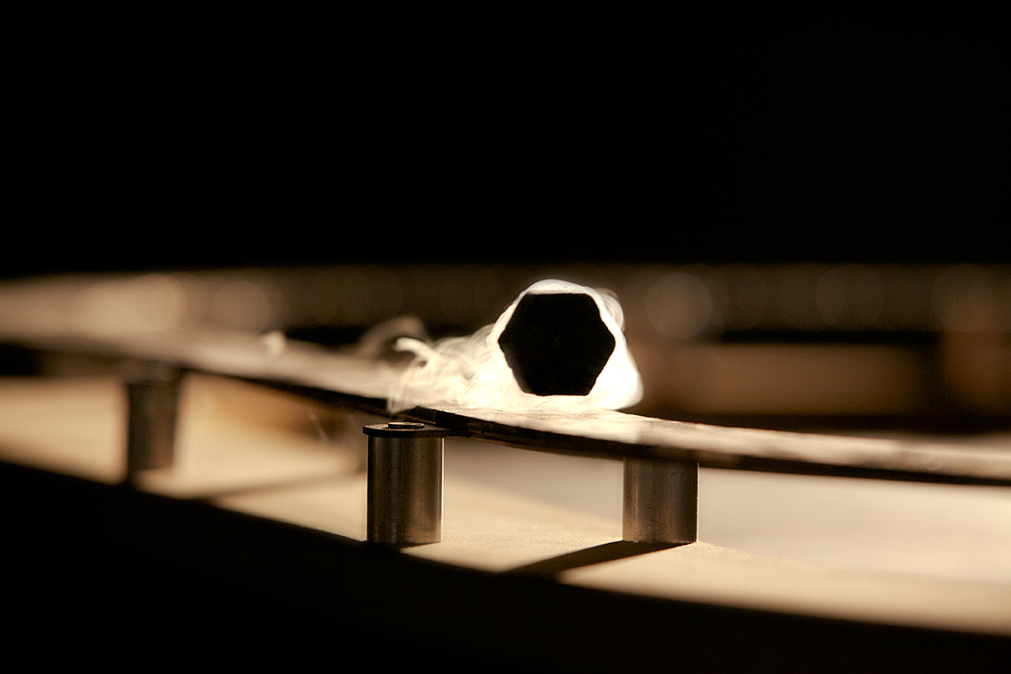
Superconductors like this pellet of the cuprate YBa2Cu3O6+x resist the influence of external magnetic fields, enabling the materials to levitate above magnets.
Courtesy of Andrea Damascelli
The key to superconductivity is to coax electrons, which normally repel one another, to pair up and form entities known as bosons. Bosons can then collectively meld into a frictionless quantum fluid. Attractive forces that create bosons, such as atomic vibrations, can normally overcome electrons’ repulsion only at cryogenic temperatures or high pressures. But the need for these extreme conditions has prevented superconductivity from finding its way into everyday devices. The discovery of cuprates raised hopes that the right atomic lattice could “glue” electrons together so firmly that they’d stay stuck even at room temperature.
Going on 40 years after Bednorz and Müller’s finding, theorists still aren’t completely sure how the glue in cuprates works, much less how to tweak the materials to strengthen it. Thus, much research in condensed matter physics is a trial-and-error hunt for crystals that can keep their electrons paired or shepherd electrons in other wondrous ways. “Condensed matter is a branch of physics that allows for serendipities,” said Kim. Such was the 2004 discovery of 2D materials.
Andre Geim and Konstantin Novoselov, working with graphite at the University of Manchester in the United Kingdom, discovered a shocking consequence of the material’s flakiness. A graphite crystal contains carbon atoms arranged into loosely bound sheets of hexagons. Theorists had long predicted that without the stabilizing influence of the stack, heat-induced vibrations would break up a one-layer sheet. But Geim and Novoselov found that they could peel off stable, atomically thin sheets with little more than Scotch tape and persistence. Graphene was the first truly flat material — a plane on which electrons can slide around but not up and down.
Hone, the Columbia physicist, discovered that the world’s thinnest material is somehow also the strongest. It was a remarkable upset for a material that theorists thought wouldn’t hang together at all.
What most intrigued physicists about graphene was how the carbon flatland transformed electrons: Nothing could slow them down. Electrons often get tripped up by the lattice of atoms through which they move, acting heavier than their textbook mass (an insulator’s immobile electrons act as if they have infinite mass). Graphene’s flat lattice, however, let electrons whiz around at a million meters per second — only a few hundred times slower than the speed of light. At that constant, blistering speed, the electrons flew as if they had no mass at all, blessing graphene with extreme (though not super) conductivity.
A whole field sprang up around the wonder material. Researchers also began to think more broadly. Could 2D flakes of other substances harbor superpowers of their own? Hone was among those who branched out. In 2009, he measured some mechanical properties of graphite’s doppelgänger, molybdenum disulfide, then passed the crystal off to two optical specialists in the Columbia lab of Tony Heinz. It was a casual move that would change the careers of everyone involved.
The molybdenum disulfide sample landed in the hands of Jie Shan, a visiting professor early in her career, and Kin Fai Mak, a graduate student. The young duo was studying how graphene interacts with light, but they had already started daydreaming about other materials. Graphene’s speedy electrons make it a fantastic conductor, but what they wanted was a 2D semiconductor — a material whose flow of electrons they could turn on and off, and which could therefore serve as a transistor.
Molybdenum disulfide was known to be a semiconductor. And Shan and Mak soon found out that, like graphite, it gained additional powers in 2D. When they pointed a laser on 3D crystals of “moly disulfide” (as they affectionally call it), the crystals stayed dark. But when Shan and Mak ripped off layers with Scotch tape, hit them with a laser, and examined them under a microscope, they saw the 2D sheets shining brightly.
Research from other groups would later confirm that well-made sheets of a closely related material reflect every last photon that hits them. “That’s kind of mind-boggling,” Mak said recently, when I met him and Shan in their shared office at Cornell. “You just have a single sheet of atoms, and it can reflect 100% of the light like a perfect mirror.” They realized that this property might lead to spectacular optical devices.
Independently, Feng Wang, a physicist at the University of California, Berkeley, made the same discovery. A 2D material that was highly reflective and a semiconductor to boot caught the community’s attention. Both groups published their findings in 2010; the papers have since received more than 16,000 citations between them. “Everybody with lasers started getting very interested in 2D materials,” Hone said.
By identifying moly disulfide as a second 2D wonder material, the two groups had made landfall on a whole continent of 2D materials. Moly disulfide belongs to a family of substances known as transition metal dichalcogenides (TMDs), in which atoms from the metallic middle region of the periodic table such as molybdenum link up with pairs of chemical compounds known as chalcogenides, such as sulfur. Moly disulfide is the only naturally occurring TMD, but there are dozens more that researchers can whip up in labs — tungsten disulfide, molybdenum ditelluride and so on. Most form weakly bound sheets, making them susceptible to the business side of a piece of tape.
The initial wave of excitement soon ebbed, however, as researchers struggled to get TMDs to do more than shine. Wang’s group, for one, fell back on graphene after finding that they couldn’t easily attach metal electrodes to moly disulfide. “That has been the stumbling block for our group for quite a few years,” he said. “Even now we are not very good at making contact.” It seemed that the main advantage of TMDs over graphene was also their biggest weakness: To study a material’s electronic properties, researchers must often push electrons into it and measure the resistance of the resulting current. But because semiconductors are poor conductors, it’s hard to get electrons in or out.
Mak and Shan initially felt ambivalent. “It was really unclear whether we should keep working on graphene or start working on this new material,” Mak said. “But since we found it has this nice property, we continued to do a few more experiments.”
As they worked, the two researchers became increasingly enchanted by moly disulfide, and by each other. Initially, their contact was professional, limited largely to research-focused emails. “Fai was often asking, ‘Where is that piece of equipment? Where did you put that?’” Shan said. But eventually their relationship, incubated by long hours and catalyzed by experimental success, turned romantic. “We just saw each other too often, literally in the same lab working on the same project,” Mak said. “The project working very well also made us happy.”
All Physics All the Time
It would take a partnership between two devoted physicists with iron discipline to bring the troublesome TMDs to heel.
Academics always came easily to Shan. Growing up in the 1970s in the coastal province of Zhejiang, she was a star student, excelling in math, science and language and earning a coveted spot at the University of Science and Technology of China in Hefei. There, she qualified for a selective cultural exchange program between China and the Soviet Union, and she jumped at the chance to study Russian and physics at Moscow State University. “When you’re a teen, you’re eager to explore the world,” she said. “I didn’t hesitate.”
Right away, she saw more of the world than she had bargained for. Visa troubles delayed her arrival in Russia by a few months, and she lost her seat in the language program. The authorities found her another course, and shortly after landing in Moscow she boarded a train and traveled 5,000 kilometers east. Three days later she arrived in the city of Irkutsk in the middle of Siberia at the onset of winter. “The advice I got was, ‘Never, ever touch anything without gloves,’” lest she get stuck, she said.
Shan kept her gloves on, learned Russian in a single semester, and came to appreciate the stark beauty of the wintry landscape. When the course ended and the snow melted, she returned to the capital to begin her physics degree, arriving in Moscow in the spring of 1990, in the midst of the breakup of the Soviet Union.
Those were chaotic years. Shan saw tanks rolling through the streets near the university as Communists tried to regain control of the government. On another occasion, just after a final exam, fighting broke out. “We could hear gunfire, and we were told to turn off the lights in the dorm,” she said. Everything, from food to toilet paper, was rationed through a coupon system. Nevertheless, Shan felt inspired by the resilience of her professors, who continued with their research despite the turmoil. “The conditions were tough, but many of the scientists had this kind of an attitude. They truly love what they do, despite what’s going on,” she said.
As the world order collapsed, Shan distinguished herself, publishing a theoretical optics paper that caught Heinz’s eye at Columbia. He encouraged her to apply, and she relocated to New York, where she occasionally helped other international students get their footing in a foreign country. She recruited Wang to work in Heinz’s lab, for instance, and shared experimental tips. “She taught me how to be patient,” he said, and “how to not get frustrated with the laser.”
Most researchers take a postdoctoral position after earning their Ph.D., but Shan joined Case Western Reserve University directly as an associate professor in 2001. Several years later, on a sabbatical, she returned to Heinz’s lab at Columbia. For once, her timing was fortuitous. She started collaborating with a charming and bright-eyed graduate student in Heinz’s group, Kin Fai Mak.
Mak had followed a different, less tumultuous path to New York City. Growing up in Hong Kong, he struggled in school, as little besides physics made sense to him. “It was the only thing I like and was actually good at, so I picked physics,” he said.
His undergraduate research at Hong Kong University of Science and Technology stood out, and Heinz recruited him to join Columbia’s booming condensed matter physics program. There, he threw himself into research, spending almost all his waking hours in the lab except for the occasional game of intramural soccer. Andrea Young, a fellow grad student (now a professor at the University of California, Santa Barbara), shared an apartment with Mak on West 113th Street. “I was lucky if I could catch him at 2 o’clock in the morning to cook some pasta and talk about physics. It was all physics all the time,” Young said.
But the good times didn’t last. Shortly after an excursion to the Amazon rainforest in Colombia with Young, Mak fell ill. His doctors weren’t sure what to make of his puzzling test results, and he got sicker. A lucky coincidence saved his life. Young described the situation to his father, a medical researcher, who immediately recognized the signs of aplastic anemia — an unusual blood condition that happened to be the subject of his own research. “It’s actually really rare to get this disease, first of all,” Mak said. “And even rarer to get a disease that your roommate’s father is an expert in.”
Young’s father helped Mak enroll in experimental treatments. He spent much of his final year of graduate school in the hospital and came close to death several times. Throughout the ordeal, Mak’s ardor for physics drove him to keep working. “He was writing PRL letters from his hospital bed,” Young said, referring to the journal Physical Review Letters. “Despite all of this, he was one of the most productive students ever,” Heinz said. “It was something of a miracle.”
Further treatments eventually helped Mak make a full recovery. Young, himself a well-known experimentalist, would later quip about his interventions, “Among friends I call it my greatest contribution to physics.”
Into the 2D Wilderness
Mak moved on to Cornell as a postdoctoral researcher in 2012, by which time Shan had already returned to Case Western. They pursued individual projects with graphene and other materials, but they also continued to unlock further secrets of the TMDs together.
At Cornell, Mak learned the art of electron transport measurements — the other main way of divining the movement of electrons, besides optics. This expertise made him and Shan a double threat in a field where researchers typically specialize in one type or the other. “Whenever I meet Fai and Jie I complain, ‘It’s unfair you guys do transport,’” Kim said. “What am I supposed to do?”
The more the duo learned about TMDs, the more intriguing they got. Researchers typically focus on one of two properties of electrons: their charge and spin (or intrinsic angular momentum). Controlling the flow of electric charge is the foundation of modern electronics. And flipping electrons’ spin could lead to “spintronics” devices that pack more information into smaller spaces. In 2014, Mak helped discover that electrons in 2D moly disulfide can acquire a special, third property: These electrons must move with specific amounts of momentum, a controllable attribute known as “valley” that researchers speculate might spawn yet a third field of “valleytronics” technology.
That same year, Mak and Shan identified another striking feature of TMDs. Electrons are not the only entities that move through a crystal; physicists also track “holes,” the vacancies created when electrons hop elsewhere. These holes can roam a material like real positively charged particles. The positive hole attracts a negative electron to form a fleeting partnership, known as an exciton, in the moment before the electron plugs the hole. Shan and Mak measured the attraction between electrons and holes in 2D tungsten diselenide and found it hundreds of times stronger than in a typical 3D semiconductor. The finding hinted that excitons in TMDs could be especially robust, and that in general electrons were more likely to do all sorts of weird things.
Merrill Sherman/Quanta Magazine
Merrill Sherman/Quanta Magazine
The couple secured positions together at Pennsylvania State University and started a lab there. Finally convinced that TMDs were worth betting their careers on, they made the materials the focus of their new group. They also got married.
Meanwhile, Hone’s team at Columbia saw graphene’s properties get even more extreme when they placed it on top of a high-quality insulator, boron nitride. It was an early example of one of the most novel aspects of 2D materials: their stackability.
Put one 2D material on top of another, and the layers will sit a fraction of a nanometer apart — no distance at all from the perspective of their electrons. As a result, stacked sheets effectively merge into one substance. “It’s not just two materials together,” Wang said. “You really create a new material.”
Whereas graphene consists exclusively of carbon atoms, the diverse family of TMD lattices brings dozens of additional elements into the stacking game. Each TMD has its own intrinsic abilities. Some are magnetic; others superconduct. Researchers looked forward to mixing and matching them to fashion materials with their combined powers.
But when Hone’s group placed moly disulfide on an insulator, the properties of the stack showed lackluster gains compared to what they had seen in graphene. Eventually they realized that they hadn’t checked the quality of the TMD crystals. When they had some colleagues stick their moly disulfide under a microscope capable of resolving individual atoms, they were stunned. Some atoms sat in the wrong place, while others had gone missing entirely. As many as 1 in 100 lattice sites had some problem, impeding the lattice’s ability to direct electrons. Graphene, in comparison, was the image of perfection, with roughly one defect per million atoms. “We finally realized that the stuff we’d been buying was complete garbage,” Hone said.
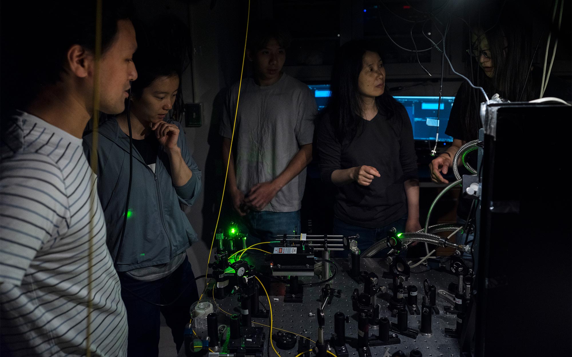
Mak and Shan oversee a group of a couple dozen students and junior researchers.
Sasha Maslov for Quanta Magazine
Around 2016, he decided to go into the business of growing research-grade TMDs. He recruited a postdoc, Daniel Rhodes, with experience growing crystals by melting powders of raw materials at extremely high temperatures and then cooling them at a glacial pace. “It’s like growing rock candy from sugar in water,” Hone explained. The new process took a month, compared to a few days for commercial methods. But it produced TMD crystals hundreds to thousands of times better than the ones for sale in chemical catalogs.
Before Shan and Mak could take advantage of Hone’s increasingly pristine crystals, they faced the unglamorous task of figuring out how to work with microscopic flakes that don’t like to accept electrons. To pump in electrons (the basis of the transport technique Mak had picked up as a postdoc), the couple obsessed over countless details: which type of metal to use for the electrode, how far from the TMD to place it, even which chemicals to use to clean the contacts. Trying out the endless ways of setting up electrodes was slow and laborious — “a time-consuming process of refining this or refining that bit by bit,” Mak said.
They also spent years figuring out how to lift and stack the microscopic flakes, which measure just tenths of millionths of a meter across. With this ability, plus Hone’s crystals and improved electrical contacts, everything came together in 2018. The couple moved to Ithaca, New York, to take new positions at Cornell, and a cascade of pioneering results came spilling out of their lab.
Breakthroughs at Cornell
“Today, everything is hard to pick up for some reason,” said Zhengchao Xia, a graduate student in Mak and Shan’s group, as the dark silhouette of a boron nitride flake threatened to peel off and fall back to the silicon surface below. The Madagascar-shaped sheet clung feebly to a hunk of graphite resembling Saudi Arabia, much as paper might cling to the crackling surface of a recently rubbed balloon. The graphite, in turn, was stuck to a gooey dewdrop of plastic attached to a glass slide. Xia used a computer interface to direct a motorized stand gripping the slide. Like an arcade-goer might maneuver a claw machine with a joystick, she gingerly lifted the stack into the air at a rate of one-fifth of a millionth of a meter per mouse click, staring intently at the computer monitor to see if she had successfully nabbed the boron nitride flake.
She had. With a few more clicks the two-layer stack came free, and Xia moved swiftly but deliberately to deposit the flakes onto a third material embedded with sprawling metal electrodes. With a few more clicks she heated the surface, melting the slide’s plastic adhesive before either of us could sneeze the microscopic device away.
“I always have this nightmare that it just disappears,” she said.
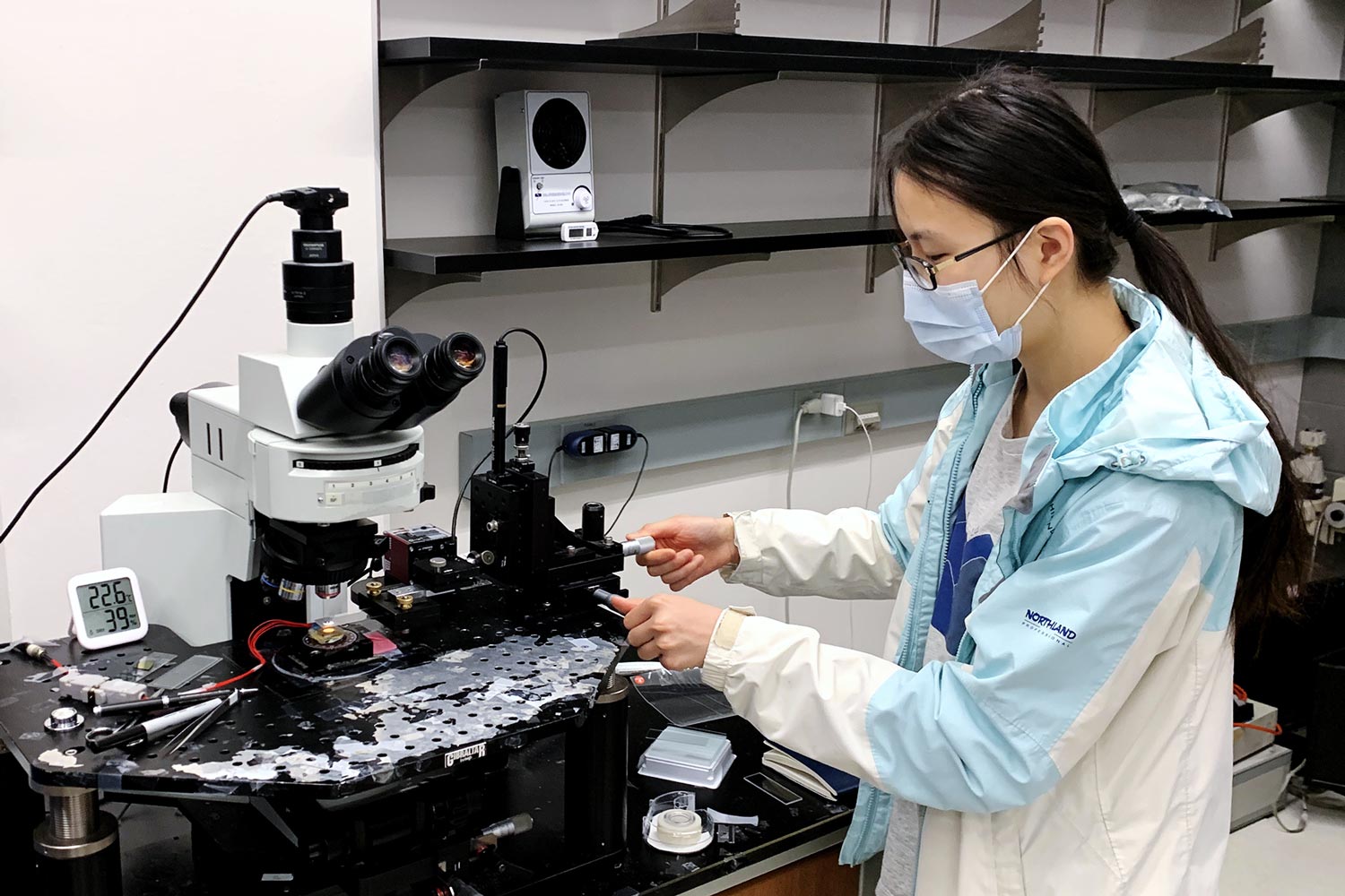
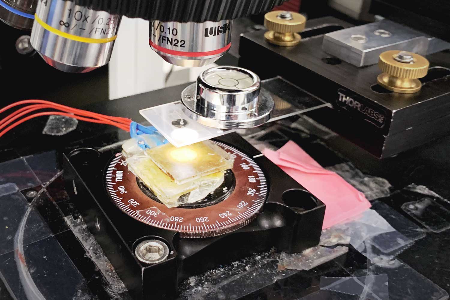
Zhengchao Xia, a graduate student in Mak and Shan’s group, uses a motorized positioning stage to stack layers of material into a new 2D device.
Charlie Wood/Quanta Magazine
From start to finish, it had taken Xia more than an hour to assemble the bottom half of a simple device — the equivalent of an open-faced PB&J. She showed me another stack she had recently put together and rattled off a few of the ingredients, which included the TMDs tungsten diselenide and moly ditelluride. One of dozens of microscopic sandwiches she has constructed and studied over the last year, this Dagwood of a device had a whopping 10 layers and took several hours to assemble.
This stacking of 2D materials, which is also done in labs at Columbia, the Massachusetts Institute of Technology, Berkeley, Harvard and other institutions, represents the realization of a long-held dream of condensed matter physicists. No longer are researchers restricted to materials found in the ground or grown slowly in a lab. Now they can play with the atomic equivalent of Lego bricks, snapping together sheets to build bespoke structures with desired properties. When it comes to assembling TMD structures, few have gone as far as the Cornell group.
Mak and Shan’s first major discovery at Cornell concerned excitons, the strongly bound electron-hole pairs they had seen in TMDs back in 2014. Excitons intrigue physicists because these “quasiparticles” may offer a roundabout way to achieve a perennial goal of condensed matter physics: room-temperature superconductivity.
Excitons play by the same funky rules as electron-electron pairs; these electron-hole pairs, too, become bosons, which lets them “condense” into a shared quantum state known as a Bose-Einstein condensate. This coherent horde of quasiparticles can display quantum traits such as superfluidity, the ability to flow with no resistance. (When a superfluid carries electric current, it superconducts.)
But unlike repulsive electrons, electrons and holes love to couple up. Researchers say this potentially makes their glue stronger. The challenges to exciton-based superconductivity lie in keeping the electron from filling the hole, and getting the electrically neutral pairs to flow in a current — all in as warm a room as possible. So far, Mak and Shan have solved the first problem and have a plan to tackle the second.
Clouds of atoms can be coaxed into forming condensates by chilling them to a hair above absolute zero with powerful lasers. But theorists have long suspected that condensates of excitons could form at higher temperatures. The Cornell group made this idea a reality with their stackable TMDs. Using a two-layer sandwich, they put extra electrons in the top layer and removed electrons from the bottom, leaving holes. The electrons and holes paired up, making excitons that are long-lived because the electrons have trouble jumping to the opposite layer to neutralize their partners. In October 2019, the group reported signs of an exciton condensate at a balmy 100 kelvins. In this setup, the excitons persisted for tens of nanoseconds, a lifetime for this type of quasiparticle. In the fall of 2021, the group described an improved apparatus where excitons seem to last for milliseconds, which Mak called “practically forever.”
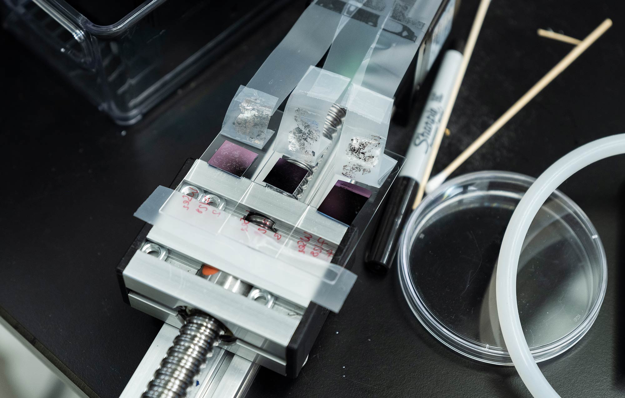
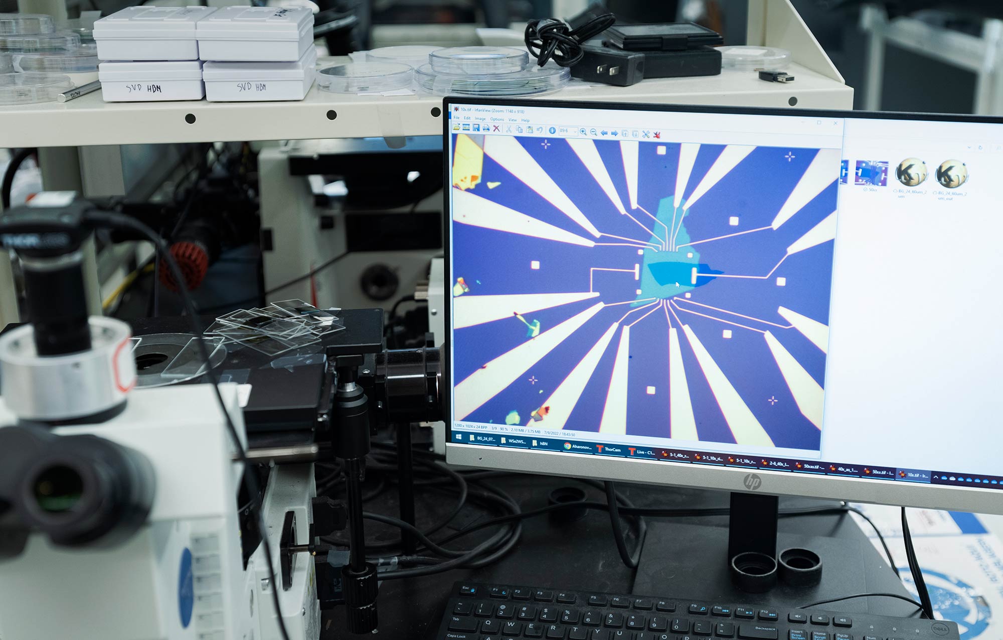
Researchers rip Scotch tape off a 3D crystal to create 2D sheets (left). They then stack these layers and attach electrodes. A microscopic image of one such device appears on a computer monitor (right).
Sasha Maslov for Quanta Magazine
The team is now pursuing a scheme concocted by theorists in 2008 for creating an exciton current. Allan MacDonald, a prominent condensed matter theorist at the University of Texas, Austin, and his graduate student Jung-Jung Su proposed making neutral excitons flow by applying an electric field oriented in a way that encourages both electrons and holes to move in the same direction. To pull it off in the lab, the Cornell group must once again grapple with their perennial enemy, electrical contacts. In this case, they have to attach multiple sets of electrodes to the TMD layers, some to manufacture the excitons and others to move them.
Shan and Mak believe they are on track to get excitons flowing at up to 100 kelvins soon. That’s a frigid room for a person (−173 degrees Celsius or −280 degrees Fahrenheit), but it’s a huge leap from the nanokelvin conditions that most bosonic condensates need.
“That will be by itself a nice achievement,” Mak said with a sly smile, “to warm up the temperature by a billion times.”
Magical Moiré Materials
In 2018, while the Cornell lab ramped up their TMD experiments, another graphene surprise launched a second 2D materials revolution. Pablo Jarillo-Herrero, a researcher at MIT and another Columbia alum, announced that twisting one layer of graphene with respect to the layer below created a magical new 2D material. The secret was to drop the upper layer such that its hexagons landed with a slight “twist,” so that they were rotated exactly 1.1 degrees against the hexagons below. This angle misalignment causes an offset between atoms that grows and shrinks as you move across a material, generating a repeating pattern of large “supercells” known as a moiré superlattice. MacDonald and a colleague had calculated in 2011 that at the “magic angle” of 1.1 degrees, the unique crystal structure of the superlattice would compel graphene’s electrons to slow and sense the repulsion of their neighbors.
Merrill Sherman/Quanta Magazine
Merrill Sherman/Quanta Magazine
When electrons become aware of each other, weird things happen. In normal insulators, conductors and semiconductors, electrons are thought to interact only with the lattice of atoms; they race around too quickly to notice each other. But slowed to a crawl, electrons can jostle each other and collectively assume an assortment of exotic quantum states. Jarillo-Herrero’s experiments demonstrated that, for poorly understood reasons, this electron-to-electron communication in twisted, magic-angle graphene gives rise to an especially strong form of superconductivity.
The graphene moiré superlattice also introduced researchers to a radical new way of controlling electrons. In the superlattice, electrons become oblivious to the individual atoms and experience the supercells themselves as if they were giant atoms. This makes it easy to populate the supercells with enough electrons to form collective quantum states. Using an electric field to dial up or down the average number of electrons per supercell, Jarillo-Herrero’s group was able to make their twisted bilayer graphene device serve as a superconductor, act as an insulator, or display a raft of other, stranger electron behaviors.
Physicists around the world rushed into the nascent field of “twistronics.” But many have found that twisting is tough. Atoms have no reason to fall neatly into the “magic” 1.1-degree misalignment, so sheets wrinkle in ways that completely change their properties. Xia, the Cornell graduate student, said she has a bunch of friends at other universities working with twisted devices. Creating a working device typically takes them dozens of tries. And even then, each device behaves differently, so specific experiments are almost impossible to repeat.
TMDs present a far easier way to create moiré superlattices. Because different TMDs have hexagonal lattices of different sizes, stacking a lattice of slightly larger hexagons over a smaller lattice creates a moiré pattern just the way angle misalignment does. In this case, because there is no rotation between the layers, the stack is more likely to snap into place and stay still. When Xia sets out to create a TMD moiré device, she said, she generally succeeds four times out of five.
TMD moiré materials make ideal playgrounds for exploring electron interactions. Because the materials are semiconductors, their electrons get heavy as they slog through the materials, unlike the frenetic electrons in graphene. And the gigantic moiré cells slow them down further: Whereas electrons often move between atoms by “tunneling,” a quantum mechanical behavior akin to teleportation, tunneling rarely happens in a moiré lattice, since supercells sit roughly 100 times further apart than the atoms inside them. The distance helps the electrons settle down and gives them a chance to know their neighbors.
Shan and Mak’s friendly rival, Feng Wang, was one of the first to recognize the potential of TMD moiré superlattices. Back-of-the-envelope calculations suggested that these materials should give rise to one of the simplest ways electrons can organize — a state known as a Wigner crystal, where mutual repulsion locks lethargic electrons into place. Wang’s team saw signs of such states in 2020 and published the first image of electrons holding each other at arm’s length in Nature in 2021. By then, word of Wang’s TMD moiré activities had already spread through the tightknit 2D physics community, and the Cornell TMD factory was churning out TMD moiré devices of their own. Shan and Mak also reported evidence for Wigner crystals in TMD superlattices in 2020 and discovered within months that electrons in their devices could crystallize in almost two dozen different Wigner crystal patterns.
At the same time, the Cornell group was also crafting TMD moiré materials into a power tool. MacDonald and collaborators had predicted in 2018 that these devices have the right combination of technical features to make them perfectly represent one of the most important toy models in condensed matter physics. The Hubbard model, as it’s called, is a theorized system used to understand a wide variety of electron behaviors. Independently proposed by Martin Gutzwiller, Junjiro Kanamori and John Hubbard in 1963, the model is physicists’ best attempt to strip the practically infinite variety of crystalline lattices down to their most essential features. Picture a grid of atoms hosting electrons. The Hubbard model assumes that each electron feels two competing forces: It wants to move by tunneling to neighboring atoms, but it’s also repulsed by its neighbors, which makes it want to stay where it is. Different behaviors arise depending on which desire is strongest. The only problem with the Hubbard model is that in all but the simplest case — a 1D string of atoms — it is mathematically unsolvable.
According to MacDonald and colleagues, TMD moiré materials could act as “simulators” of the Hubbard model, potentially solving some of the field’s deepest mysteries, such as the nature of the glue that binds electrons into superconducting pairs in cuprates. Instead of struggling with an impossible equation, researchers could set electrons loose in a TMD sandwich and see what they did. “We can write down this model, but it’s very difficult to answer lots of important questions,” MacDonald said. “Now we can do it just by doing an experiment. That’s really groundbreaking.”
To build their Hubbard model simulator, Shan and Mak stacked layers of tungsten diselenide and tungsten sulfide to create a moiré superlattice, and they attached electrodes to dial up or down an electric field passing through the TMD sandwich. The electric field controlled how many electrons would fill each supercell. Since the cells act like giant atoms, going from one electron to two electrons per supercell was like transforming a lattice of hydrogen atoms into a lattice of helium atoms. In their initial Hubbard model publication in Nature in March 2020, they reported simulating atoms with up to two electrons; today, they can go up to eight. In some sense, they had realized the ancient aim of turning lead into gold. “It’s like tuning chemistry,” Mak said, “going through the periodic table.” In principle, they can even conjure up a grid of fictitious atoms with, say, 1.38 electrons each.
Next, the group looked to the hearts of the artificial atoms. With more electrodes, they could control the supercells’ “potential” by making changes akin to adding positive protons to the centers of the giant synthetic atoms. The more charge a nucleus has, the harder it is for electrons to tunnel away, so this electric field let them raise and lower the hopping tendency.
Mak and Shan’s control of the giant atoms — and therefore the Hubbard model — was complete. The TMD moiré system lets them summon a grid of ersatz atoms, even ones that don’t exist in nature, and smoothly transform them as they wish. It’s a power that, even to other researchers in the field, borders on magical. “If I were to single out their most exciting and impressive effort, that’s the one,” Kim said.
The Cornell group quickly used their designer atoms to settle a 70-year-old debate. The question was: What if you could take an insulator and tweak its atoms to turn it into a conducting metal? Would the changeover happen gradually or abruptly?
With their moiré alchemy, Shan and Mak carried out the thought experiment in their lab. First they simulated heavy atoms, which trapped electrons so that the TMD superlattice acted like an insulator. Then they shrank the atoms, weakening the trap until electrons became able to hop to freedom, letting the superlattice become a conducting metal. By observing a gradually falling electrical resistance as the superlattice acted increasingly like a metal, they showed that the transition is not abrupt. This finding, which they announced in Nature last year, opens up the possibility that the superlattice’s electrons may be able to achieve a long-sought type of fluidity known as a quantum spin liquid. “That may be the most interesting problem one can tackle,” Mak said.
Almost at the same time, the couple lucked into what some physicists consider their most significant discovery yet. “It was actually a total accident,” Mak said. “Nobody expected it.”
When they started their Hubbard simulator research, the researchers used TMD sandwiches in which the hexagons on the two layers are aligned, with transition metals atop transition metals and chalcogenides atop chalcogenides. (That’s when they discovered the gradual insulator-to-metal transition.) Then, serendipitously, they happened to repeat the experiment with devices in which the top layer had been stacked backward.
As before, the resistance started falling as electrons began to hop. But then it plunged abruptly, going so low that the researchers wondered if the moiré had begun to superconduct. Exploring further, though, they measured a rare pattern of resistance known as the quantum anomalous Hall effect — proof that something even weirder was going on. The effect indicated that the crystal structure of the device was compelling electrons along the edge of the material to act differently from those in the center. In the middle of the device, electrons were trapped in an insulating state. But around the perimeter, they flowed in one direction — explaining the super-low resistance. By accident, the researchers had created an extremely unusual and fragile type of matter known as a Chern insulator.
The quantum anomalous hall effect, first observed in 2013, usually falls apart if the temperature rises above a few hundredths of a kelvin. In 2019, Young’s group in Santa Barbara had seen it in a one-off twisted graphene sandwich at around 5 kelvins. Now Shan and Mak had achieved the effect at nearly the same temperature, but in a no-twist TMD device that anyone can re-create. “Ours was a higher temperature, but I’ll take theirs any day because they can do it 10 times in a row,” Young said. That means you can understand it “and use it to actually do something.”
Mak and Shan believe that, with some fiddling, they can use TMD moiré materials to build Chern insulators that survive to 50 or 100 kelvin. If they’re successful, the work could lead to another way to get current flowing with no resistance — at least for tiny “nanowires,” which they may even be able to switch on and off at specific places within a device.
Exploration in Flatland
Even as the landmark results pile up, the couple shows no signs of slowing down. On the day I visited, Mak looked on as students tinkered with a towering dilution refrigerator that would let them chill their devices to temperatures a thousand times colder than what they’ve worked with so far. There’s been so much physics to discover at “warmer” conditions that the group hasn’t had a chance to thoroughly search the deeper cryogenic realm for signs of superconductivity. If the super fridge lets the TMDs superconduct, that will answer yet another question, showing that a form of magnetism intrinsic to cuprates (but absent from TMDs) is not an essential ingredient of the electron-binding glue. “That’s like killing one of the important components that theorists really wanted to kill for a long time,” Mak said.
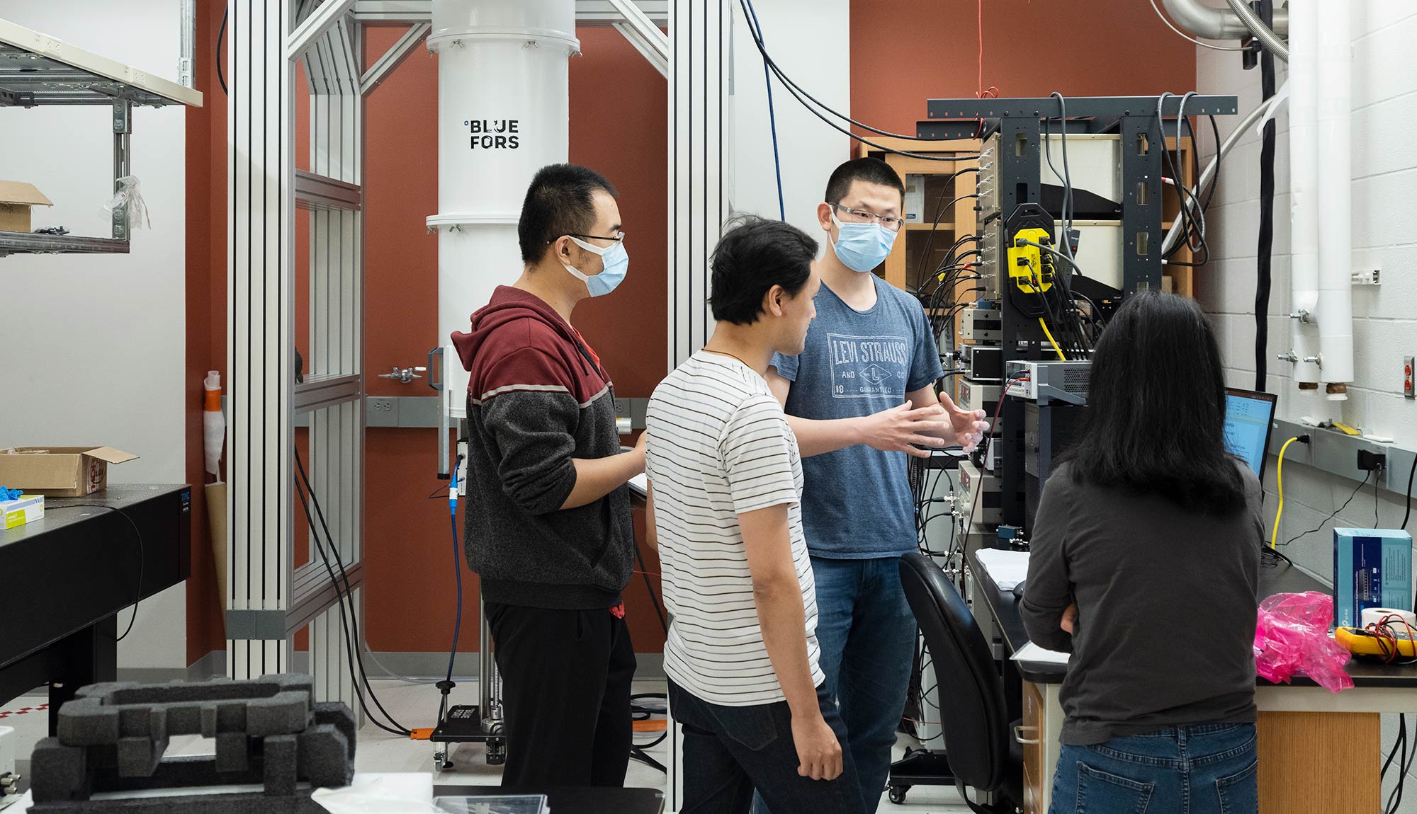
Lab members chat near their new Blue Fors dilution refrigerator.
Sasha Maslov for Quanta Magazine
He and Shan and their group haven’t even begun to experiment with some of the funkier TMDs. After spending years inventing the equipment needed to move around the continent of 2D materials, they’re finally gearing up to venture beyond the moly disulfide beachhead they landed on back in 2010.
The two researchers attribute their success to a culture of cooperation that they absorbed at Columbia. The initial collaboration with Hone that introduced them to moly disulfide, they say, was just one of the many opportunities they enjoyed because they were free to follow their curiosity. “We didn’t have to discuss” their plans with Heinz, the head of their lab, Shan said. “We talked to people from other groups. We did the experiments. We even wrapped things up.”
Today they foster a similarly relaxed environment at Cornell, where they oversee a couple dozen postdocs, visiting researchers and students, all of whom are largely free to do their own thing. “Students are very smart and have good ideas,” Mak said. “Sometimes you don’t want to interfere.”
Their marriage also makes their lab unique. The two have learned to lean into their personal strengths. Besides an abundance of creativity as an experimentalist, Shan possesses a careful discipline that makes her a good manager; as the three of us talked, she frequently nudged “Professor Fai” back on track when his enthusiasm for physics pushed him too deep into technicalities. Mak, for his part, enjoys toiling alongside the early-career researchers, both inside and outside the lab. He recently started rock climbing with the group. “It seems like their lab is their family,” said Young. Shan and Mak told me they achieve more together than they could alone. “One plus one is more than two,” Mak said.
The devices they’re building may also stack up to be more than the sum of their parts. As researchers join TMD sheets together to create excitons and moiré superlattices, they speculate about how the new ways of domesticating electrons might supercharge technology. Even if pocket-ready superconductivity remains elusive, Bose-Einstein condensates could lead to ultra-sensitive quantum sensors, and better control of Chern-like insulators could enable powerful quantum computers. And those are just the obvious ideas. Incremental improvements in materials science often add up to radical applications few saw coming. The researchers who developed the transistor, for instance, would have struggled to predict smartphones powered by billions of microscopic switches stuffed into a chip the size of a fingernail. And the scientists who endeavored to fashion glass fibers that could carry light across their lab bench could not have foreseen that 10,000-kilometer undersea optical fibers would someday link continents. Two-dimensional materials may evolve in similarly unpredictable directions. “A really new materials platform generates its own applications as opposed to displacing existing materials,” said Heinz.
While driving me to the Ithaca bus stop, Shan and Mak told me about a recent (and rare) vacation they took to Banff, Canada, where they once again displayed their knack for stumbling onto surprises through a blend of effort and luck. They had spent days trying — in vain — to spot a bear. Then, at the end of the trip, on their way to the airport, they stopped to stretch their legs at a botanical reserve and found themselves face to face with a black bear.
Similarly, with condensed matter physics, their approach is to wander around together in a new landscape and see what shows up. “We don’t have much theoretical guidance, but we just fool around and play with experiments,” Mak said. “It can fail, but sometimes you can bump into something very unexpected.”
Corrections: August 17, 2022
An earlier version of this article misstated the full name of the university where Kin Fai Mak did undergraduate research, as well as the current title of Andrea Young.
